
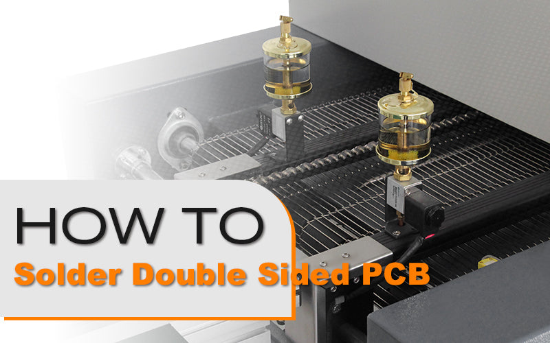
As electronic products continue to advance in functionality and require smaller, more compact designs, there is a need for double-sided circuit boards to provide additional space to meet consumers' demands for lightweight, portable, and stylish devices. So the question arises: How to solder double-sided circuit boards?

Reflow soldering a double-sided PCB requires careful planning and execution to ensure proper soldering and avoid component damage or misalignment.
Here's 3 ways to reflow soldering a double-sided PCB:
1. Reflow soldering using red glue first and then solder paste:
Application: This process is generally suitable when the components are relatively dense and the components on one side are mostly different in height. Red glue is usually applied. In particular, large components have high gravity and may fall off after reflow soldering. The red glue will become stronger when heated.
Process: Incoming material inspection-->Screen-printed solder paste on side A of PCB-->SMT-->AOI or QC inspection-->Reflow soldering on side A-->Flip board-->Silk-printed red glue or dispensing red glue on side B of PCB Dispensing red glue (special attention: whether it is dispensing red glue or screen printing red glue, the red glue is applied to the middle part of the component. Do not let the red glue contaminate the pad of the PCB component foot, otherwise the component foot cannot be soldered. )-->Patch-->Drying-->Cleaning-->Testing-->Repair.
Note: Be sure to solder the solder paste surface first, and then dry the red plastic surface, because the drying temperature of red plastic is relatively low and can be cured at about 180 degrees. If you dry the red plastic surface first, it will easily cause components to fall out during the subsequent operations on the solder paste surface.
2. Reflow soldering of solder paste on both sides:
Application: Generally, when there are a lot of components on both sides, and there are large ICs or BGAs with dense pins on both sides, you can only apply solder paste to mount them. If you apply red glue, it will easily cause the IC pins and pads to be out of alignment.
Process: Incoming material inspection-->Screen-printed solder paste on side A of PCB-->Patch-->QC or AOI inspection-->Reflow soldering on side A-->Flip board-->Silk-printed solder paste on side B of PCB- ->Patch-->QC or AOI inspection-->Reflow soldering-->Cleaning-->Inspection-->Rework.
Here the details,
- Prepare the PCB: Make sure the PCB is clean and free of any debris, flux residues, or oxidation. Use a brush or compressed air to clean the surface.
- Apply Solder Paste: Apply solder paste to the pads on oneside of the PCB using a stencil. Ensure that the solder paste is evenly distributed and covers all the pads accurately.
- Place Components: Place the components on one side of the PCB. Ensure that the components are correctly oriented and aligned with their respective pads.
- Preheat: Preheat the PCB to a temperature slightly below the reflow temperature to prevent thermal shock to the components. This preheating phase helps in reducing the temperature gradient during reflow.
- Reflow Soldering: Transfer the PCB to the reflow oven or reflow soldering equipment. Follow the temperature profile recommended by the solder paste manufacturer. The reflow process involves gradually heating the PCB to the reflow temperature, holding it at that temperature for a specified duration, and then gradually cooling it down.
- Apply Solder Paste: Once the first side is soldered, carefully flip the PCB and apply solder paste to the pads on the other oneside of the PCB using a stencil.
- Second Side Component Placement: Place components on the second side. Ensure proper alignment and orientation of the components.
- Reflow Second Side: Repeat the reflow soldering process for the second side of the PCB, following the same temperature profile used for the first side.
- Cooling: Allow the PCB to cool down gradually to room temperature. Rapid cooling can cause thermal stress and potentially damage the components or solder joints.
- Inspection: After cooling, inspect the solder joints on both sides of the PCB. Ensure that all components are properly soldered and there are no solder bridges, cold joints, or other defects.
- Touch-up: If any defects are found, perform touch-up soldering using a soldering iron and solder wire. Be careful not to overheat the components during touch-up.
- Cleaning: Clean the PCB thoroughly to remove any flux residues or contaminants using an appropriate cleaning solution.
- Testing: Finally, test the PCB to ensure that all components are functioning correctly and that there are no electrical or mechanical issues.

Note: In order to avoid large components falling off when passing through the B side, when setting the reflow soldering temperature, the temperature of the molten soldering zone in the lower temperature zone should be set slightly lower than the temperature in the upper temperature zone by 5 degrees(After the solder paste melts, its melting point when dissolved again is 5 degrees higher than the melting point of the solder paste.). In this way, the tin below will not melt again and cause the components to fall off. Some people suggest blowing cold gas across the bottom of the substrate so that the temperature at the bottom never reaches the melting point during secondary reflow. However, it is a bit difficult to implement cold air. It seems to be a better idea to use a heat insulation board (mica sheet) on the bottom of the circuit board.
3. Use solder pastes with different melting points. The melting point of the solder paste used during the second reflow is lower than that of the second reflow.
Reflow soldering double-sided PCBs requires attention to detail and proper coordination to ensure successful soldering on both sides without damaging components. Following the recommended temperature profiles and handling procedures will help achieve good soldering results.
The above is a summary of several methods from experts. If you have a better way, please leave a message below or contact me rose@itechsmt.com, I’m happy to discuss with you.